Choose timezone
Your profile timezone:
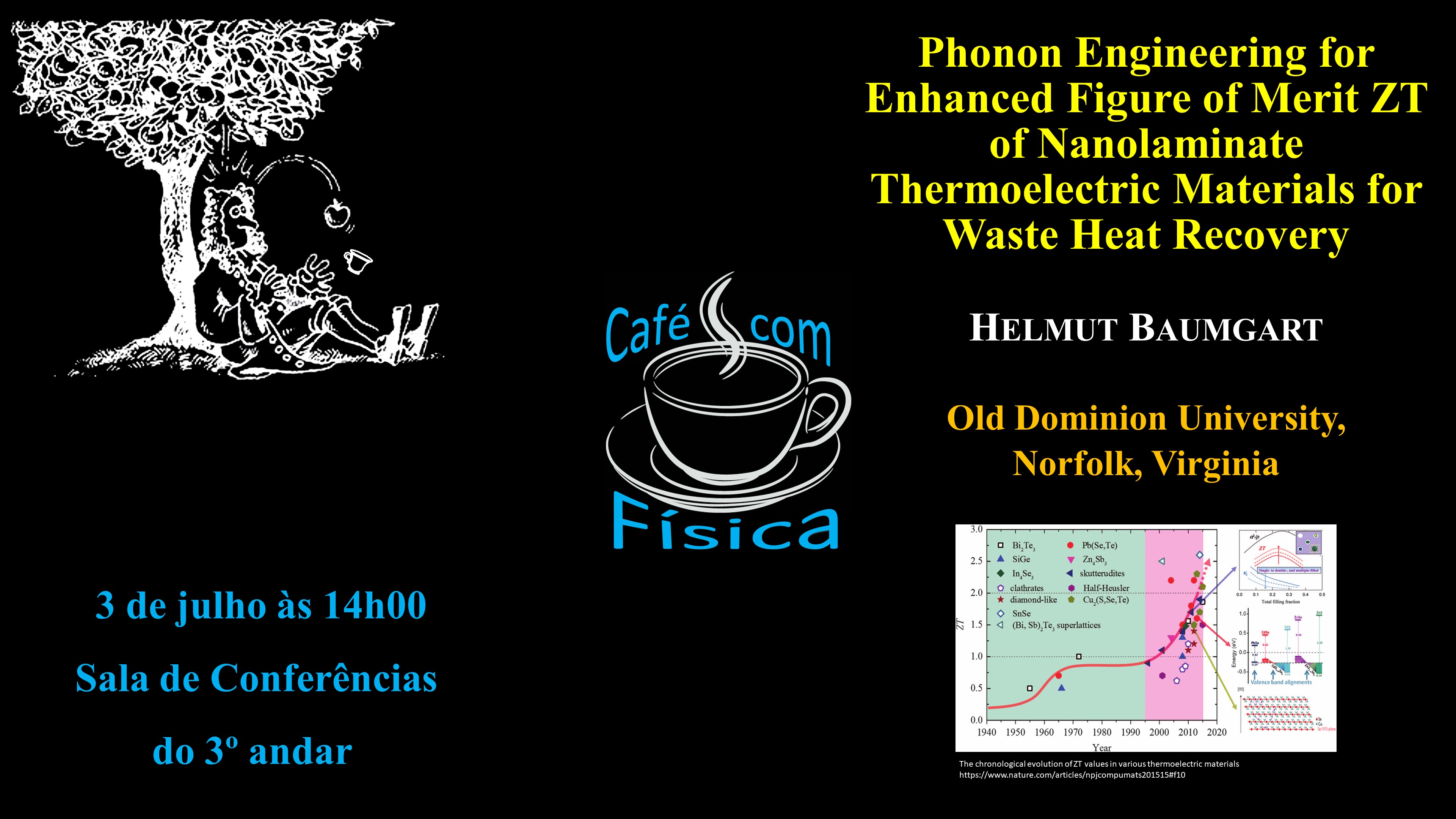
Thermoelectric materials and generators contribute to save energy by converting waste heat into electricity based on the Seebeck effect and thus constitute an alternate green renewable energy technology. High efficiency thermoelectric materials have attracted considerable attention because of their application potential in power generation and refrigeration systems. The efficiency of thermoelectric materials is expressed by the figure of merit (ZT), ZT = S2σT/ (kl + ke). It is observed that higher thermoelectric efficiency can be obtained by increasing the electron conductivity and reducing the thermal conductivity. In the quest to enhance ZT values, a key strategy involves reduction in thermal conductivityk, resulting from phonon scattering by numerous interfaces in low dimensional structures. A decrease of thermal conductivity could be achieved by a low dimensional superlattice structure, due to the quantum confinement or phonon scattering. 1
Recently promising advances have been achieved with phononic crystal (PnC) nanostructures in thermoelectric materials, because the thermal conductivity of PnC samples is lower compared to non-patterned thermoelectric samples due to phonon-boundary scattering. In this study we report on the successful synthesis of PbTe and PbSe thermoelectric layers on patterned porous silicon substrates by a thermal ALD system. PbTe/PbSe nanolaminates grown on porous silicon membranes have higher Seebeck coefficients than the ones grown on regular planar silicon wafers. The higher Seebeck values result from the lower thermal conductivity k in porous structures, which in turn lead to a higher figure of merit ZT. We demonstrate the feasibility to enhance the figure of merit ZT further by modulating the size and periodicity of the pattern and the thickness of the thermoelectric film in relation to the mean free path (MFP) of the phonons of the thermoelectric material. In our study PbTe and PbSe thin films and nanolaminates were synthesized by Atomic Layer Deposition (ALD) technology on regular planar silicon wafers and on macro-porous silicon templates. ALD is a surface saturating, self-limiting, absolutely conformal thin film synthesis technique reacting two pulsed precursors that enable film growth of one atomic layer per growth cycle. Lead bis(2,2,6,6-tetramethyl-3,5-heptanedionato) (Pb(C11H19O2)2), (trimethylsilyl) telluride ((Me3Si)2Te) and (trimethylsilyl) selenide ((Me3Si)2Se) were employed as the chemical ALD precursors for lead, tellurium and selenium, respectively. The surface morphology observations indicate Volmer–Weber (VW) growth mechanism of PbTe/PbSe nanolaminates during the thermal ALD deposition process rather than classic layer-by-layer growth. The ALD PbTe/PbSe nanolaminates exhibited complete surface coverage on planar bulk silicon wafers and also inside the pores of microporous silicon membranes. For the case of porous Si templates, the Seebeck measurements in both the horizontal and vertical directions revealed significant enhancement in Seebeck coefficients for PbTe/PbSe nanolaminates synthesized inside strictly periodic lithographically defined porous silicon membranes.
Reference
1-X. Chen, P. Lin, K. Zhang, H. Baumgart, B. Geist, and V. Kochergin, ECS J. Solid State Sci. Technol. 5 (9), P503 (2016).
Filipe Veloso e Pedro Costa